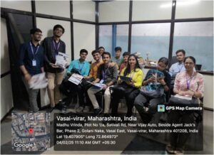
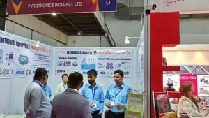
| Name of Event | Industrial Visit to Janyu Technologies Pvt Ltd. , Vasai |
| Date of Event | February 4th, 2025 |
| Faculty In Charges | Ms. Aarti Naik Mr. Vinaykumar Singh |
| Objective of the Visit: | 1. Understanding Robotics Applications– Observing the role of robotics in industries such as manufacturing, healthcare, and logistics. 2. Exposure to Advanced Technologies– Learning about AI, machine learning, IoT, and automation in robotics. 3. Industry Interaction– Engaging with experts to explore career opportunities, industry trends, and challenges. |
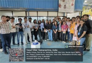
| Event Details: | Our visit to Janyu Technologies Pvt Ltd. commenced at 10:00 AM, with us assembling at the company premises in Vasai East, Mumbai. It began with an introductory session by the technical team, highlighting the company’s profile, core operations, and ongoing research in robotics and automation.
We were then guided through various departments where they observed real-time applications of robotics in industries such as manufacturing, healthcare, and logistics. Demonstrations included AI-driven automation, IoT-enabled devices, and advanced robotic systems used in industrial settings.
Industry experts provided insights into career opportunities and skill requirements in the field of robotics, offering valuable guidance for students looking to build careers in emerging technologies. It concluded with an interactive Q&A, allowing us to clarify doubts and gain deeper knowledge of industry challenges. |
| Outcome of the Visit: | ● Students gained practical exposure to robotics applications and automation processes. ● They developed an understanding of AI, machine learning, and IoT in industrial automation. ● Students were able to interact with industry experts and gain insights into career prospects and technological advancements. ● They observed workplace discipline, teamwork, and the importance of innovation in technology-driven industries. ● The visit helped students bridge the gap between theoretical learning and real-world industrial practices |
Glimpse of Industrial Visit: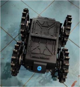
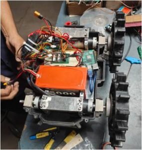
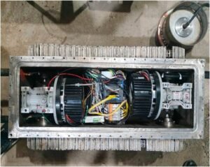
IoT-enabled devices, and Advanced robotic systems
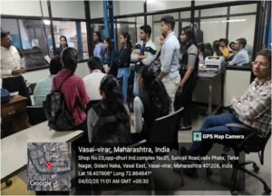
Janyu Technologies Pvt Ltd. from inside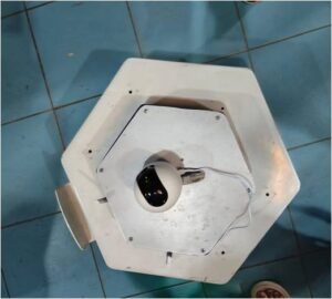
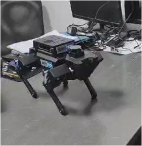
AI-driven automation, and Advanced robotic systems
| Particulars | Description |
| Activity | Exploring MEMS Technology at IIT Bombay Nanofabrication Lab |
| Sub activity | Understanding Micro-Electro-Mechanical Systems (MEMS) in Real-world Applications |
| Activity Level | Departmental |
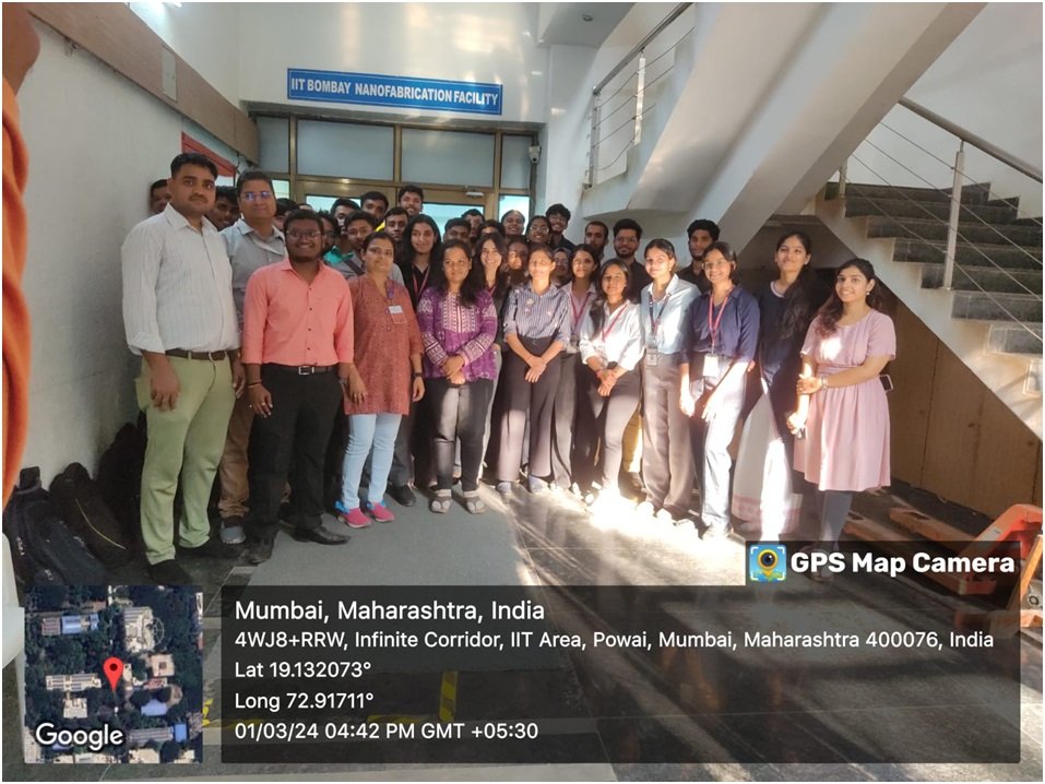
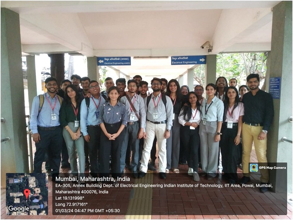
| Title | Industrial Visit to IIT Bombay Nanofabrication Lab |
| Organized by | Electronics And Computer Science department |
| Venue | IIT Bombay, Powai |
| Date | 01/03/24 |
| Time | 2.30 pm Onwards |
| Objective of event | Provide students with practical insights into MEMS technology by experiencing its applications at the cutting-edge Nanofabrication Lab in IIT Bombay. Enhance understanding and interest in MEMS, a key component of the curriculum in the eighth semester. |
| Targeted Participants | Fourth year |
| List of Distinguished guest present during the opening ceremony. | Mrs.Samita Bhandari(Assistant Professor,ECS) Mr. Vinay Singh (AssistantProfessor, ECS) |
| Speaker | – |
| Total Participants | 29 |
| Content of the activity | The industrial visit to IIT Bombay’s Nanofabrication Lab proved to be an enriching experience for the fourth-year students of the Electronics and Computer Science Department. The event aimed to bridge the gap between theoretical knowledge and practical application, focusing on MEMS technology, a crucial aspect of the academic curriculum. The participants were guided through the advanced facilities of the Nanofabrication Lab, gaining firsthand exposure to the intricate processes involved in manufacturing micro-electro-mechanical systems. The visit provided a unique opportunity for students to witness the real-world applications of MEMS, fostering a deeper understanding and appreciation for the subject. The interactive sessions and demonstrations conducted by experts from IIT Bombay left a lasting impact, igniting curiosity and enthusiasm among the participants as they explored the fascinating realm of MEMS technology. |
| Methodology used | Industrial Visit |
| Particulars | Description |
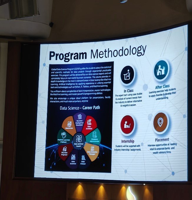
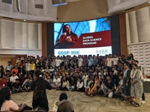
| Activity: | Field visit to BSE to learn about the Global Data Science Program and network with industry professionals. |
| Sub Activity: | Field Visit (one day) |
| Activity level: | ECS Department level |
| Title: | Field Visit to BSE(Bombay Stock Exchange) |
| Organized by: | ECS Department SLRTCE |
| Venue: | BSE, Fort, Mumbai |
| Date: | 11th September 2023 |
| Time: | 3:00 pm am to 6:30 pm |
| Objective of event: |
|
| Outcome of event: |
|
| Targeted Participants: | Faculties of SLRTCE, TE ECS students |
| Total Participants: | 35 |
| Speaker: | NA |
| Content of the activity: | Learn about the data science field and its applications in the financial industry. Explore the Global Data Science Program at BSE, including its curriculum, teaching methodology, and industry partnerships. Gain insights into the career opportunities available to graduates of the program. Network with industry professionals and other students interested in pursuing a career in data science. Leave with a deeper understanding of the data science field and the skills and knowledge required to be a successful data scientist.. |
| Methodology used: |
|

| Particulars | Description |
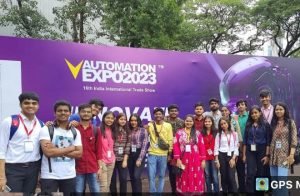
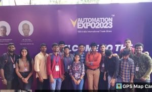
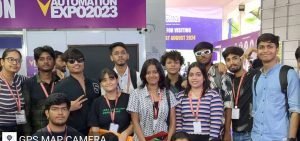
| Activity: | Field/Exposure visit to Automation Expo to know more about the companies showcasing their products and evolving technologies. |
| Sub Activity: | Field Visit (one day) |
| Activity level: | Intra Dept.(ECS Dept) |
| Title: | Field Visit Automation Expo |
| Organized by: | ECS Department SLRTCE |
| Venue: | Automation Expo, NESCO, Goregaon |
| Date: | 26th August 2023 |
| Time: | 10:30 am to 3pm |
| Objective of event: |
|
| Outcome of event: | 1. This visit has given a brief idea to students about the pace at which the world around them is progressing. They are now well versed with this “hi-tech” era. Automation Expo 2023 has fetched information from all aspects of technology in bulk. Not only in technical terms but a clue about companies and set-ups involved in making our lives easier through their inventions, was known to them. |
| Targeted Participants: | Faculties of SLRTCE, SE, TE ECS students |
| Total Participants: | 41 |
| Speaker: | NA |
| Content of the activity: | The visit provided a platform for participant’s to connect with professionals, entrepreneurs, and researchers working in the field of innovation and technology transfer. This networking opportunity can lead to potential collaborations and partnerships in the future. |
| Methodology used: |
|
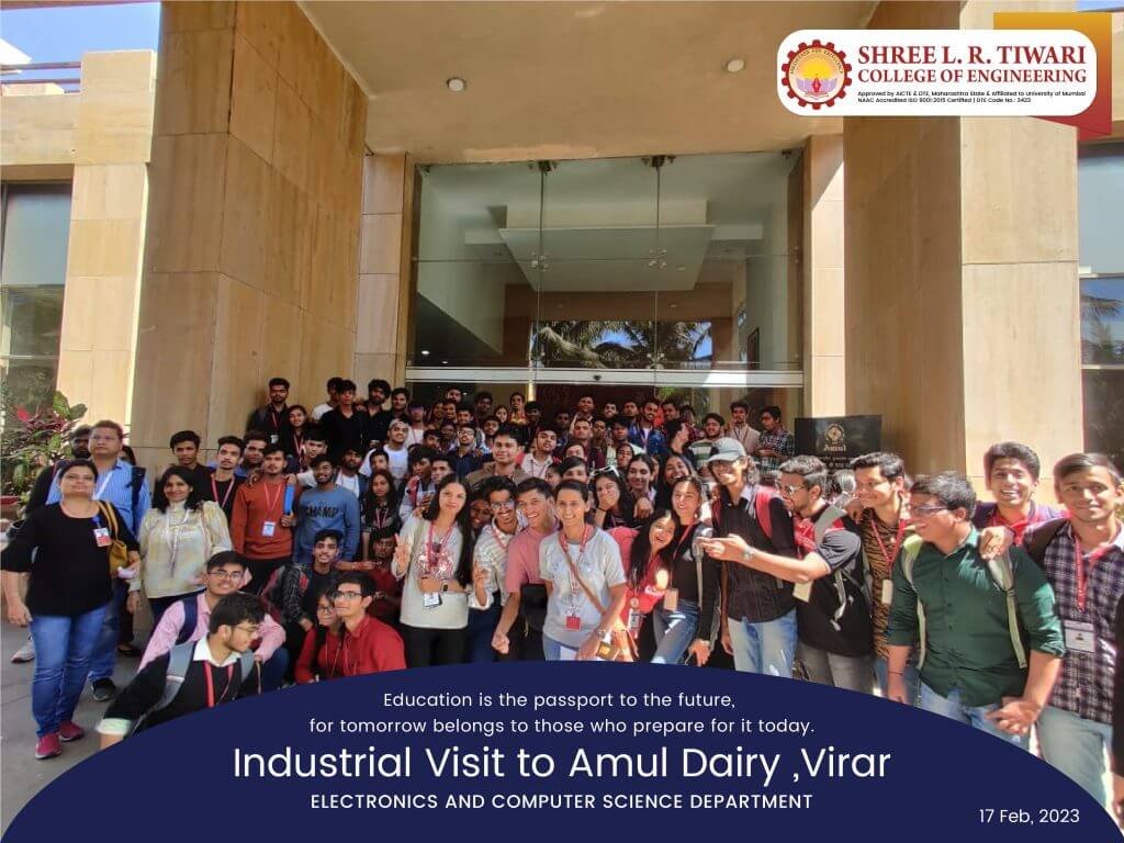
| Name of Event | Industrial Visit to Visit to Amul Dairy ,Virar |
| Date of Event | 17/02/2023 |
| Faculty In Charges | Ms. Aarti Naik Mrs. Samita Bhandari Mrs. Rashmi Maheshwari Mr. Vinay kumar Singh |
| Objective of the visit : |
|
| Event Details : | We arrived at AMUL at 10:00 AM. After that we gathered at the front gate and visited various sections of AMUL .we started with the animation movie for showing glimpse of Amul dairy from its beginning at Anand district at auditorium of dairy memorial. It also gave introduction of company profile and its present functioning in dairy industry for different milk products. The Technical team has explained automation of dairy through presentation containing many functional block diagrams and existing computerized controlled machineries. |
| Outcome of the Visit : |
|
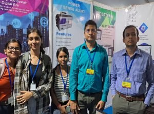
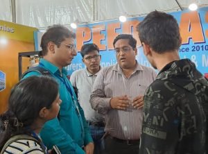
| Name of the Event: | INDUSTRIAL AUTOMATION EXPO 2022 |
| Date of the Event: | 12thSeptember, 2022 |
Faculty In charge:
– Prof. Vinaykumar Singh (Department of Electronics & Computer Science)
– Prof. Aarti Naik (Department of Electronics & Computer Science)
Objective of the visit:
The visit to Industrial Automation Expo 2022 aimed at acquainting the students of
Electronics Engineering with different upcoming ideas and innovations, that can create
revolutionary progress in this era of Technology. Moreover, to make the theoretical concepts
more resolved for the students, this visit was organized by the college faculty. To get
information about various manufacturing companies, their products and the technology
involved in making was one of the objectives. An initiative by the professors of the department
helped the students know more and more about the newness of technology, scope of the field
and areas of better job opportunities.
Event Details:
This event took place at the, Hitendra Thakur Appa ground, Vasai (E), Mumbai. The event
was scheduled from 10th September, 2022 to 12th September, 2022. Industrial Automation
Expo, South East Asia’s biggest show, extends a platform to many leading industries and
companies to showcase their products and evolving technologies that help them survive in the
domestic and global markets and sustain a better position due to intensifying competition.
The students of SLRTCE walked in at 12 p.m. after the registrations being completed at the
entrance. Then, they were free to explore the entire exhibition which was huge and phenomenal
with over 100+ exhibitors. Students came to know more about the companies they had just
heard of. Every second stall was an introduction to something new in the field of technology.
All the brands and companies present there were a step forward from each other and are
dominating with their ideas globally.
This show was also a platform to students from different colleges who could exhibit their final
year projects to the visitors.
Some companies are interested in providing internships and training to students for gaining
practical experience and knowledge.


Outcome of the Visit:
This visit has a given a brief idea to students about the pace at which the world around them is
progressing. They are now well versed with this “hi-tech” era. Automation Expo 2017 has fetched
information from all aspects of technology in bulk. Not only in technical terms but a clue about
companies and set-ups involved in making our lives easier through their inventions, was known to them.
| Name of the Event: | Virtual Industry Visit – Techfest. |
| Date of the Event: | 29th Dec 2020 – 07th Jan 2021. |
| Location of the Event: | Online Zoom platform. |
| Organized by: | IIT Bombay. |
On the 29th December 2020, the Techfest was organized by IIT Bombay which focused on giving the industrial knowledge to all the students through the online platform Zoom. The event lasted 10 days long with 10 different industrial visits. Every student was requested to select any 3 visits, best suited according to her interest and degree pursuing.
Some of the companies are listed below: –
- Johnson & Johnson.
- Nestle.
- ArcelorMittal.
- Maggie.
The speaker was called from the top authority of every company for each day. The very well explained all the detailed working of their industry right from the scratch. The speaker talked the job opens and as well as the responsibilities of joining as an industrial expert in any domain. Students learned all the important aspects of industrial working. At the end there was a brainstorming and information exchange session was followed and e-certificate was provided to all the students as soon as they completed their quiz. Altogether, it was a great learning experience with great knowledge exchange.
Date of Visit: 16/03/2019
Venue: IIT-Bombay, Powai.
Timing: 9am to 12pm
Objectives:
- To see the nanofabrication setup.
- To understand the fabrication processes for MEMS devices.
- Practical explanation for theoretical concepts.
- For better understanding of processes.
Organized by:
Samita Bhandari (Asst. Professor- Department of Electronics Engineering).
Persons Involved:
- Abhijit Somnathe (HOD-Department of Electronics Engineering).
- Madhuri Kadam (Asst. Professor- Department of Electronics and Telecommunication Engineering).
- BE ETRX students .
Event Details:
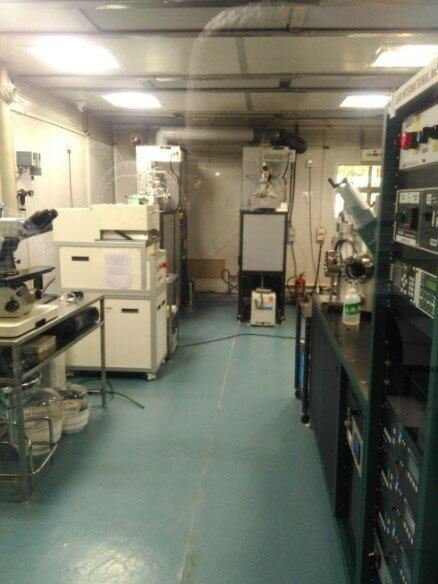
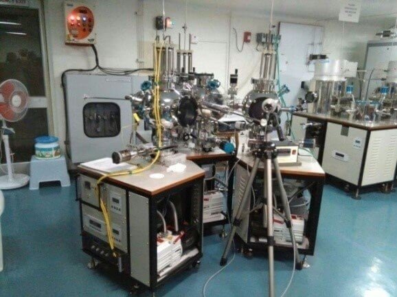
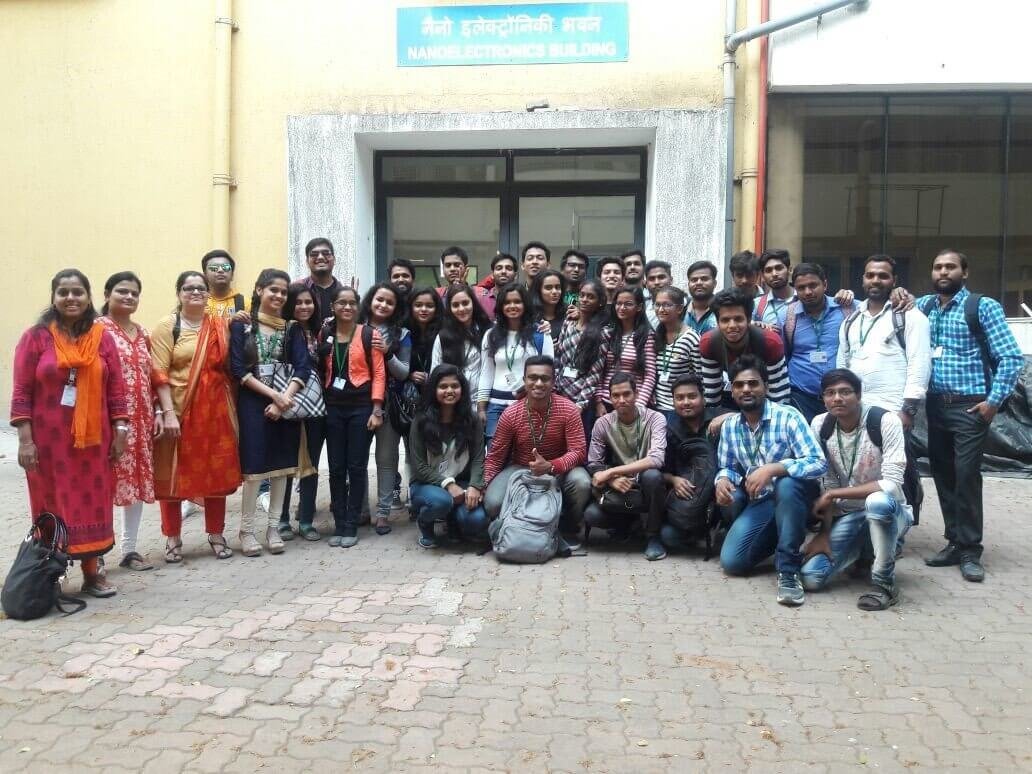
A visit to IIT-Bombay Nanoelectronics department was organised by the faculty of Shree L. R. Tiwari College of Engineering for the students. IIT-Bombay has a set up for the nanofabrication processes for research purpose. And hence this visit was organised to have a brief idea about the theoretical concepts. Students were asked to report sharp at 9am at the main gate of IIT-Bombay. After completing the formalities, everyone reached the nanoelectronics building. There the students were divided into groups of 10. Each group was made to visit the various labs one by one accompanied by a research scholar there. Following topics were covered from the syllabus.
Deposition systems (CVD, ALD, PVD):
| PVD Depositions: | Silicon Nitride, Silicon Oxide, Silicon Oxy Nitride and Amorphous Silicon. |
| Types of substrates: | 2”,4”,8”, small pieces of wafers- Si, glass, Quartz. |
| Temperature: | Room temperature to 380 degree Celsius. |
| Process gas used: | SiH₄, N₂O, CF₄, Ar, He, H₂, N₂, NH.₃ |
| Instrument Provider: | Oxford Instruments. |
| Gases available: | SiH₄, N₂O, CF₄, Ar, He, |
Molecular Beam Epitaxy:
MBE takes place in high vacuum or ultra-high vacuum (10-8 Pa). The most important aspect of MBE is slow deposition rate (typically less than 1000 nm per hour), which allows the films to grow epitaxially. The slow deposition rates require proportionally better vacuum to achieve the same impurity levels as other deposition techniques.
Furnaces for oxidation, diffusion and annealing (2-inch, 4 inch):
During semiconductor device fabrication, thin film growth and deposition steps typically occur more number of times than any other process. These are often critical processes that require careful thickness and quality control. For example, during silicon transistor fabrication, growth of thin film SiO₂ is generally required immediately after the RCA clean process. This oxide can be grown on the Si wafer surface using different process that define its growth rate and quality. Whatever is the chosen process, maintaining the tight control of the process conditions and minimizing contamination on the wafer surface during the growth process is critical for final device performance. Hence, separate process-based oxide growth furnaces are needed for the same.
Etch tools (STS RIE, Etch Centura and Edge Isolation tool):
While a lithography process is used to write micrometre/nanometre-sized patterns on a resist layer, a different technique is needed to transfer those patterns from the resist onto the main layer on the semiconductor wafer. Wet etching and dry etching are the most commonly used processes to achieve this goal. Dr. etch usually refers to material removal or patterning using a chemically reactive plasma. When a lithographic patterned sample is introduced into this plasma, ionic species bombard and chemically react with the exposed areas, while the resist patterned areas are left protected. This method is anisotropic whereas wet etch is isotropic in nature. As a result, this method is preferable.
Lithography Tools:
IITBNF has multiple optical lithography tools with different dimension limits. They also have a laser writer system that is capable of producing mask plates with micrometre sized (patterns for use in optical lithography tools. The best resolution at IITBNF (< 20nm) is achieved through the state-of-the-art e-beam lithography tool. This tool can also be used for silicon dioxide and metal deposition using its electron beam induced deposition (EBID) feature. For both optical and e-beam tools, resist spinners dedicated to different types of resists are available with capabilities to process 2”, 4” and 8” wafers. All lithography tools housed in separate clean rooms with tight control over temperature and lighting conditions.
Plasma Immersion Ion Implanter:
As CMOS device gate length has shrunk to 45nm, the short channel effects (SCE) becomes very severe. To reduce SCE, one of the solutions is to make very shallow S/D junctions. For the same, implant energy is less than 2keV is required, where commercial Ion Beam Implanters have several issues like beam current instabilities at low voltages. PIII is very suitable for ion energy even at 200V operation. This system uses BF₃ and PH₃ gases for Boron (p type) and Phosphorous (n type) implants in Si wafers.
Event Outcomes:
Students have understood the concepts better and have come to know about the actual practical set up of nanofabrication processes. A visual idea was obtained by this visit about the Clean Room and Si wafers.


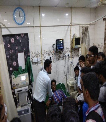
VENUE:Global Hospital, near Ramdev park Mira Road (E).
DATE: 24/08/2018
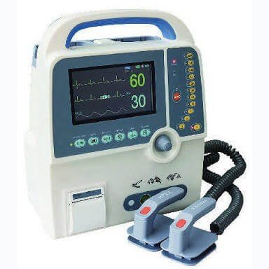
Students of TE ETRX SLRTCE visited hospital for study and demonstration of some instruments like ECG machine, blood pressure measurement equipment and Defibrillator.
They observe various function and application of instruments and they demonstrated how it works practically
- ECG Machine
Electrocardiography (ECG or EKG) is the process of recording the electrical activity of the heart over a period of time using electrodes placed over the skin. These electrodes detect the tiny electrical changes on the skin that arise from the heart muscle’s electrophysiological pattern of depolarizing and repolarizing during each heartbeat. It is very commonly performed to detect any cardiac problems. In ECG machine reading it shoes amount of oxygen in body and various parameter etc.
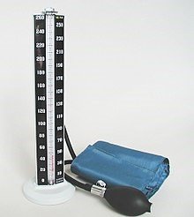
- Blood pressure measurement
The auscultatory method (from the Latin word for “listening”) uses a stethoscope and a sphygmomanometer. This comprises an inflatable (Riva-Rocci) cuff placed around the upper arm at roughly the same vertical height as the heart, attached to a mercury or aneroid manometer. The mercury manometer, considered the gold standard, measures the height of a column of mercury, giving an absolute result without need for calibration and, consequently, not subject to the errors and drift of calibration which affect other methods.useof mercury manometers is often required in clinical trials and for the clinical measurement of hypertension in high-risk patients, such as pregnant women. A cuff of the appropriate size is fitted smoothly and also snugly, then inflated manually by repeatedly squeezing a rubber bulb until the artery is completely occluded. It is important that the cuff size is correct: undersized cuffs record too high a pressure; oversized cuffs may yield too low a pressure. Usually three or four cuff sizes should be available to allow measurements in arms of different size. Listening with the stethoscope to the brachial artery at the antecubital area of the elbow, the examiner slowly releases the pressure in the cuff
- Defibrillator
Defibrillation is a treatment for life-threatening cardiac dysrhythmias, specifically ventricular fibrillation (VF) and non-perfusing ventricular tachycardia (VT). A defibrillator delivers a dose of electric current (often called a countershock) to the heart. Although not fully understood, this would depolarize a large amount of the heart muscle, ending the dysrhythmia. Subsequently, the body’s natural pacemaker in the sinoatrial node of the heart is able to re-establish normal sinus rhythm. In contrast to defibrillation, synchronized electrical cardioversion is an electrical shock delivered in synchrony to the cardiac cycle. Although the person may still be critically ill, cardioversion normally aims to end poorly perfusing cardiac dysrhythmias, such as supraventricular tachycardiawe understood that Defibrillator is used only when there is emergency When the patients heart stops working, shock is given to trigger the heart otherwise pacemaker is used.


Faculty In charge:
- Tanvi Thakur (Department of Electronics)
- Rohini Jadhav (Department of Electronics)
Objective of the visit:
The visit to Automation Expo 2018 aimed at acquainting the students of Electronics Engineering with different upcoming ideas and innovations, that can create revolutionary progress in this era of Technology. It is the largest Automation & Instrumentation exhibition. It is an ideal platform for the Indian and global automation industry to converge and exhibit the cutting-edge technologies, advancements, systems, and services. Moreover, to make the theoretical concepts more resolved for the students, this visit was organized by the college faculty. To get information about various manufacturing companies, their products and the technology involved in making was one of the objectives. An initiative by the professors of the department helped the students know more and more about the newness of technology, scope of the field and areas of better job opportunities.
Event Details:
This event took place at the Bombay Exhibition Centre, Goregaon (E), Mumbai. The event was scheduled from 29th August, 2018 to 1st September, 2018. Automation Expo, South East Asia’s biggest show, extends a platform to many leading industries and companies to showcase their products and evolving technologies that help them survive in the domestic and global markets and sustain a better position due to intensifying competition.
The students of SLRTCE walked in at 11 a.m. after the registrations being completed at the entrance. Then, they were free to explore the entire exhibition which was huge and phenomenal with over 250+ exhibitors. Students came to know more about the companies they had just heard of. Every second stall was an introduction to something new in the field of technology. Here is a list of few out of many companies:
- BHOLANATH PRECISION ENGINEERING PVT. LTD.: They are the only company in India that manufacture Motors. Their factory is at Shahpur, Thane while their office is located at Bhandup, Mumbai.
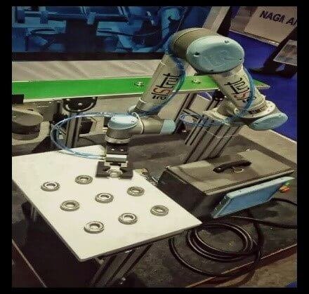
- UNIVERSAL ROBOTS.: They are involved in the manufacturing of 6 axes collaborative industrial robot (cobot) arm to mimic the range of motion of a human arm.
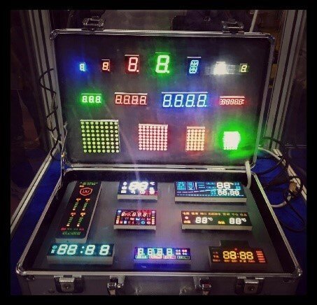
- ELECTRONIC SWITCHES: They specialise in big display indicators, digital counters, proximity switches, level sensors, etc. This company is based in Nashik.
- COMPUCARE: These are manufacturers and dealers of CCTVs, LED display board, production monitoring systems, safety solutions, etc. Their office is in Vadodara and their set up extends into cities like Ahmedabad, Surat, Mumbai, Bangalore.
- TAC AUTOMATION PVT. LTD.: They specialise in HMI, PLCs, Inverters, Servo Drives, etc. They are located in Delhi.
- TAMRON INDIA PVT. LTD.: This Industry is in Haryana. As per their tagline, they provide eyes for industries. In other words, they manufacture high quality Industrial Lenses.
- PCB POWER: It is an online PCB specialist company located in Gandhinagar, Gujrat. This company designs PCBs as per the requirement posted by the customer online on their website pcbpower.com. They do allow Industrial visits for college students.
- MENZEL VISION AND ROBOTICS PVT. LTD.: Based in Mumbai, they design Machine Vision products Apart from these companies, organizations like Nanjing Wotian Technology Co. Ltd. (China), Qinhuangdao Jialong Glass Co. Ltd.(China), Taiwan Association of Machinery Industry (Taiwan), Puls (Singapore) and other such organizations from neighbouring countries were also a part of this meet.
All the brands and companies present there were a step forward from each other and are dominating with their ideas globally. This show was also a platform to students from different colleges who could exhibit their final year projects to the visitors. Some companies are interested in providing internships and training to students for gaining practical experience and knowledge. They are listed as follows:
- Bholanath Precision Engineering Pvt.Ltd., Bhandup
- Dynalog (India) Limited., Mumbai.
Outcome of the Visit:
This visit has a given a brief idea to students about the pace at which the world around them is progressing. They are now well versed with this “hi-tech” era. Automation Expo 2017 has fetched information from all aspects of technology in bulk. Not only in technical terms but a clue about companies and set-ups involved in making our lives easier through their inventions, was known to them.


| Name of Event | Visit to IITB NANOFABRICATION LAB |
| Date of Visit | 17/03/2017. |
| Venue: | IITB Powai ( Elecrical Engg.dept) |
| Timing In: | 2pm |
| Timing Out: | 5pm |
Objectives:
- To observe nanofabrication setup.
- To understand various fabrication processes for MEMS devices .
- To give practical knowledge to students about processes which they have studied theoretically in classroom.
Persons involved:
- Prof.SamitaBhandari.(Asst.Professor ETRX):
Role – Organizer of the visit, planning ,taking permission from college&IITB, coordinating with students. - Prof.ManjiriGogate
- Prof.PragatiDiwedi
- Students of final year ETRX.
Event Details:
- Reached to the lab at 2pm.In three batches their volunteers explained all the departments one by one. Following points are covered from the syllabus.
Fabrication:
- Deposition systems (CVD,ALD,PVD)
- http://www.cen.iitb.ac.in/slotbooking/SOP/166_SOP.pdf
- http://www.cen.iitb.ac.in/slotbooking/GLIMPSE/166_GLIMPSE.pdf
- http://www.cen.iitb.ac.in/slotbooking/SOP/199_SOP.pdf
- Molecule Bam Epitaxy (GaAs/InGaAs)Molecular beam epitaxy takes place in high vacuum or ultra-high vacuum (10-8 Pa). The most important aspect of MBE is the slow deposition rate (typically less than 1000 nm per hour), which allows the &ilms to grow epitaxially. The slow deposition rates require proportionally better vacuum to achieve the same impurity levels as other deposition techniques.
- Furnaces for oxidation ,diffusion and annealing(2 inch,4inch) During semiconductor device fabrication, thin film growth and deposition steps typically occur more number of times than any other process. These are often critical processes that require careful thickness and quality control. For example, during silicon (Si) transistor fabrication, growth of a thin film of silicon dioxide (SiO2) is generally required immediately after the RCA clean process. This oxide can be grown on the Si wafer surface using different processes that define its growth rate and quality. Whatever the chosen process, maintaining tight control of process conditions and minimizing contamination on the Si wafer surface during the growth process is critical for final device performance. Hence, separate process-based oxide growth furnaces are needed for the same.
- Etch tools (STSRIE, EtchCentura & Edge isolation tool) While a lithography process is used to ‘write’ micrometer/nanometer-sized patterns on a resist layer, a different technique is needed to transfer these patterns from the resist onto the main layer on the semiconductor wafer. Wet etching & dry etching are the most commonly used processes to achieve this goal. Dry etch usually refers to material removal or patterning using a chemically reactive plasma. When a lithographically patterned sample is introduced into this plasma, ionic species bombard and chemically react with the exposed areas, while the resist-patterned areas are left protected. This method of pattern transfer from resist to the main layer using dry etch technique is anisotropic, whereas wet etch processes are typically isotropic in nature. As a result, dry etching is the preferred process for pattern transfer of small dimensions (≤ 10μm) and is often one of the critical steps in a semiconductor device fabrication run.
- Rapid thermal annealing.
- http://www.cen.iitb.ac.in/slotbooking/SOP/164_SOP.pdf
- Lithography tools.
- IITBNF has multiple optical lithography tools with different pattern dimension limits. We also have a laser writer system that is capable of producing mask plates with micrometre-sized patterns for use in the optical lithography tools. The best resolution at IITBNF (< 20 nm) is achieved through our state-of-the-art e-beam lithography tool: Raith 150 Two. This tool can also be used for in-situ silicon dioxide and metal deposition using its electron beam induced deposition (EBID) feature. For both optical & e-beam tools, resist spinners dedicated to different types of resists are available with capabilities to process 2”, 4” & 8” wafers. All lithography tools are housed in separate clean rooms with tight control over temperature, humidity & lighting conditions.
- Plasma immersion ion implaner.
As CMOS device gate length has shrunk to 45nm, the short channel effects (SCE) become very severe. To reduce SCE one of the solution is to make very shallow S/D junctions. For the same, we require implant energy less than 2KeV, where commercial Ion Beam Implanters have several issues like beam current instabilities at low voltages. PIII is very suitable for ion energy even at 200V operation. This system uses BF3 and PH3 gasses for Boron (ptype) and Phosphorus (n-type) implants in Si wafers.
- Gas injection system.
Event outcomes
- Students come to know about actual practical set up of fabrication of nanodevices/ MEMS devices. They can visualize silicon wafers, cleanroom.
PR manager Ranjana Gupta given information about various training courses for students . For interested students we can give apportunity to student to do work with after some formalities.
Scope of Improvement
- Simulation and characterization lab visit.
- Visit to nanosniff company IITB.